
- The Nanorobotics XY-stages from Klocke Nanotechnik are small enough for an assembly onto every existing SEM/FIB sample stage
- They offer sub-Nanometer resolution in movement
- They offer sub-micron stitching accuracy
- Their hardware and software is fully compatible to the Nanoworkbench application packages from Klocke Nanotechnik
- The e-beam lithography application can be expanded later e.g. by a Nano-Probing,
Nano-Cutting or Nano-Cleaning application package operating in the same control System.
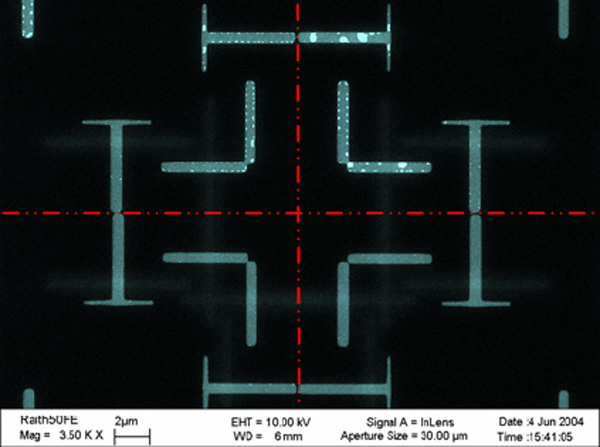
- Stitching accuracy around 500 nm with 20, 30 or 40 mm range
- High vacuum feedthrough and cable set for SEM operation
- Network controller with Ethernet communication
- Power supply and sub-rack housing
- Universal lithography sample holder
- Typical sample size up to 30x 30 mm2
- Small dimensions to fit in every electron microscope
- High vacuum compatible
- 20 mm or 30 mm stroke versions for x- and y-axis available
- Compatible to RAITH lithography software
- Expandable by Nanorobotics Manipulators, e.g. for Nano-Probing, Nano-Cutting or Nano-Cleaning
- Live Image Positioning for sample stage and manipulators
- Move the tip by a simple mouse click in the Live Image Positioning Module
XY-positioning and stitching improvements for conventional SEM based
lithography solutions by piezoelectric sub-stage assembly
Raith GmbH
Download PDF
Learn more
Download PDF