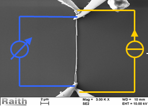

- With the Nanoworkbench from Klocke Nanotechnik probing is very fast, easy and secure.
- Possible applications are measurement of currents and voltages in 2, 3 or 4 point geometry.
- The stationary in-SEM assembly of the Nanoworkbench allows NanoProbing on any position of big wafers without moving the probe tips away.
- The Live Image Positioning module provides a simple point and click solution.
- The Nanofinger® operating as Scout allows a fast and secure automatic approach of all probes to the sample, also on isolators. The Nanofinger® tip can also be used as one of the electrical probes.
- Automatic macros and absolute positioning in superior precision allow to program measuring processes in closed loop with any feedback signal (Nanofinger®, current, force, etc)
- 2, 3 and 4 probe geometry
- the tip of the Nanofinger® operating as Scout can also be used for electrical probing
- customized tips available
- 1 nm tip movement resolution
- repeatability better than 50 nm
- 20 mm tip stroke in xy, 10 mm in z-direction
- low-resistivity low-noise shielded cable sets from tip to COAX connectors outside of the chamber
- Nano Probing is an application package of the Nanoworkbench
- Also available as a standalone module
- In situ nanomanipulation system for electrical measurements in SEM
M. Noyong, U. Simon, A. Rosenberger, V. Klocke et. al.
Meas. Sci. Technol. 18 (2007) N84–N89
Download PDF - Generation and electrical contacting of gold quantum dots,
G. Schmid & T. Reuter & U. Simon & M. Noyong et al,
Colloid Polym Sci. DOI 10.1007/s00396-008-1866-2,Springer-Verlag 2008, 6pp), IOP publishing
Download PDF - Nanomanipulation measurement and PIC simulation of field-emission properties from a single crystallized silicon nano-emitter
T.C. Cheng, K.H.Hsu et al.
Nanotechnology 18 (2007) 225503 (6pp), IOP publishing
Download PDF - Single Device Characterization by Nano-probing to Identify Failure Root Cause
Chao-Chi Wu, Jon C. Lee, et al.
Taiwan Semiconductor Manufacturing Company, Ltd.
Download PDF - Manipulation of Carbon Nanotubes inside Field-Emission ScanningElectron Microscope
Seong Chu Lim, Keun Soo Kim, Kay Hyeok An, Shinje Cho, Jae-Eun Yoo, Won Bong Choi and Young Hee Lee
Download PDF - An electromechanical material testing system for
in situ electron microscopy and applications
Yong Zhu and Horacio D. Espinosa
Download PDF - A microelectromechanical load sensor forin situ electron and x-ray
microscopy tensile testing of nanostructures
Yong Zhu, N. Moldovan and Horacio D. Espinosa
Download PDF
This application package is part of the Nanoworkbench
