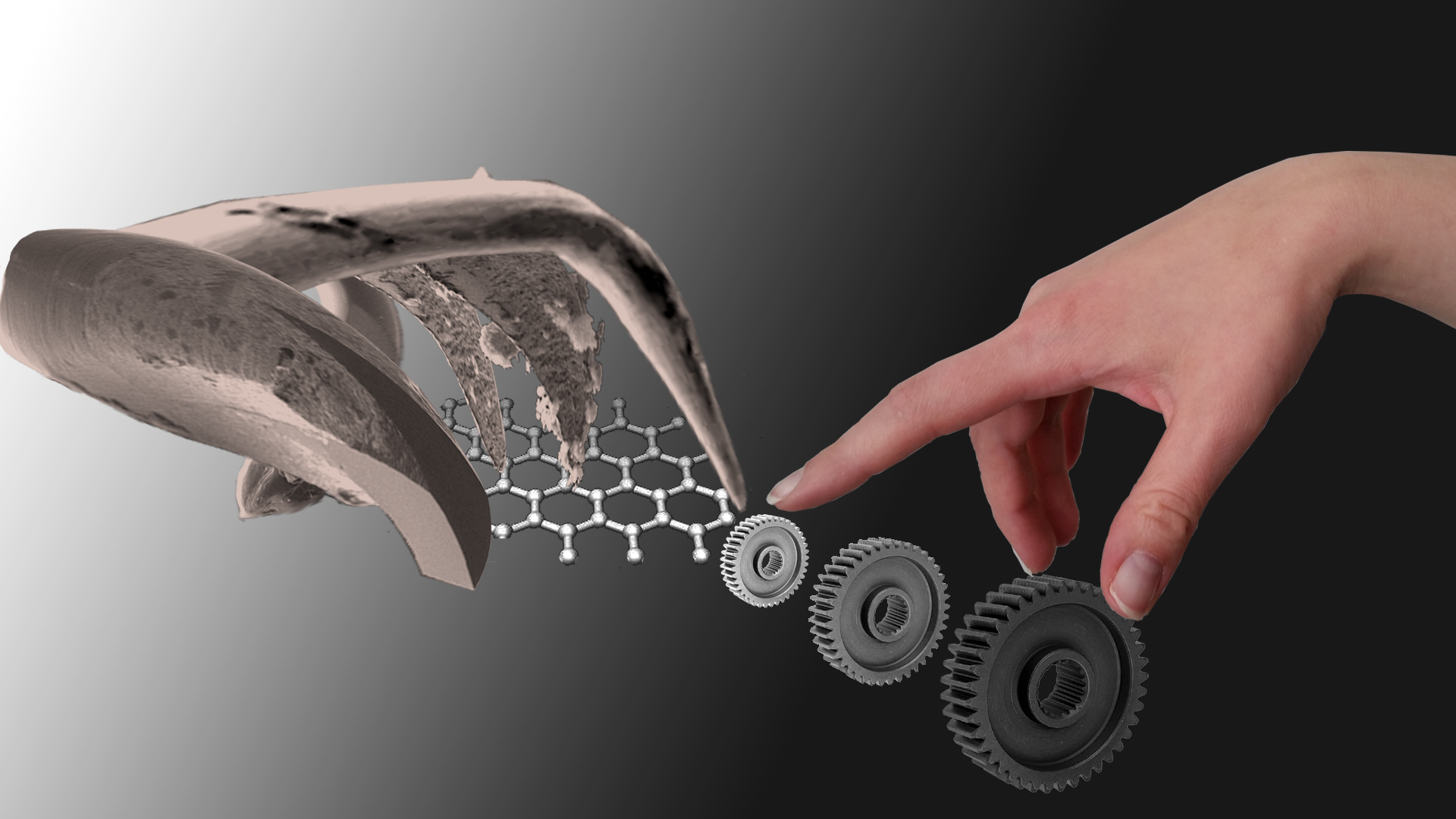
Micro production
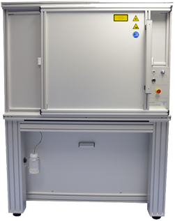
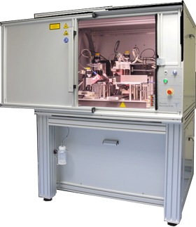
The usage of our Nanorobotics series in combination with more than 200 components allows configuring plenty of different solutions like a construction kit. These systems can have different size and complexity, but mostly they are about 100-times more precise then other solutions. Examples therefore are medium sized configurations like ultra-precise Profilometers, Micro tensile machines or Wafer-Prober – or big systems like our Micro Production System or the Universal Testing Benches. Advantage: Configuration of solutions, instead of development!These systems include plenty of different options that can only be summarized here by a few examples. More information is available on request.
The Nanoworkbench
Our Nanorobotics extends Electron or Ion Microscopes from analytical instruments to material processing systems. This page is the entry to a group of complete systems. All applications are based on our absolute positioning high performance Nanorobotics manipulators. Once installed in a SEM or FIB they can be expanded by several different modules to form application oriented turnkey solutions. This modular design allows the usage of one basic investment for several different applications. Plenty of further descriptions are available on request.
3d Nanofinger
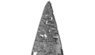
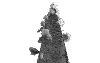
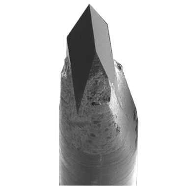
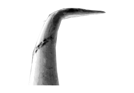
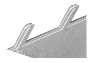
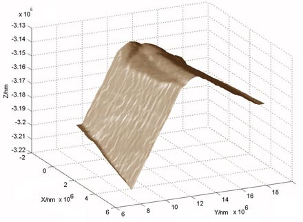
The “Nanofinger®” sensor is a small MEMS device that detects the distance between a probe tip and a sample. The Nanofinger® sensor is driven by a special high speed electronics that reacts with a bandwidth of several KHz. The Nanofinger® sensor is moved towards a sample in closed loop with 1 nm increments until it reaches the desired signal value (e.g. at 75% amplitude). At this moment the position of the stage that moves this sensor is stored as coordinate data. The Nanofinger® sensor s removed again and then moved aside for the next approach, at any time in closed loop with 1 nm increments.
Nanorobotics
The basis of Nanotechnology is micro- or nano positioning. Piezoelectric crystals achieve high resolution down to the atomic scale. Drawback of this technique is the limited stroke of only a few µm.
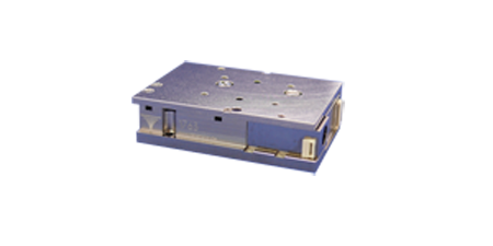
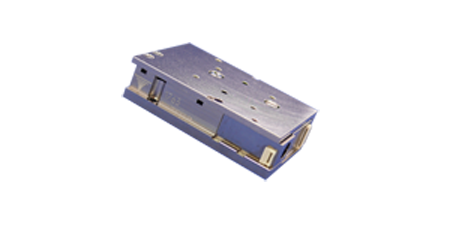
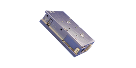
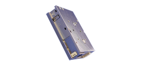
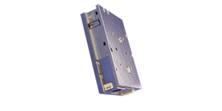
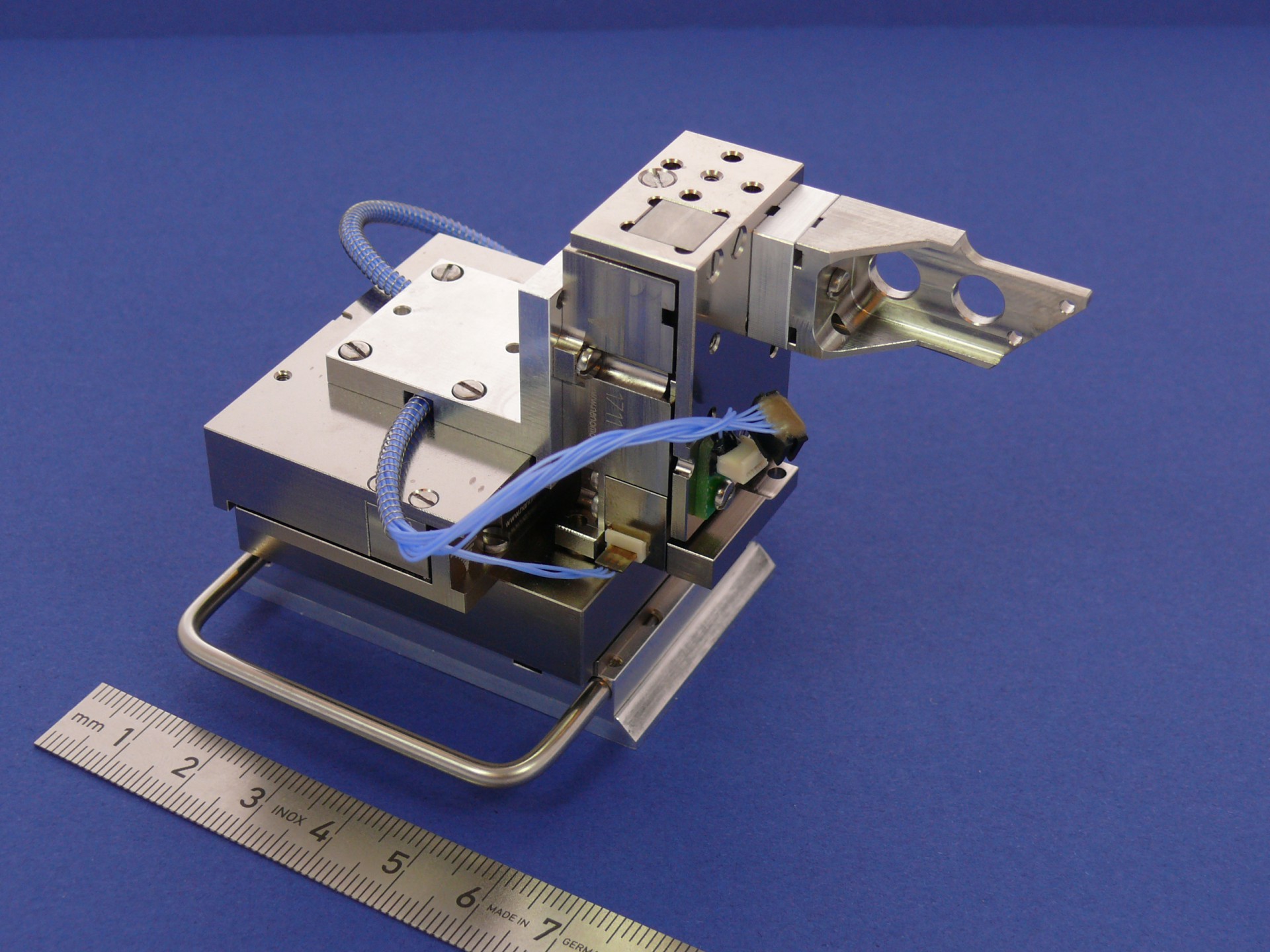
This drawback is overcome by the patented Nanomotor: It has a positioning stroke up to some centimeters while operating with atomic resolution and thus builds a bridge over eight orders of magnitude, see its very small dimensions shown


