Versions
Mobile version
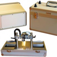
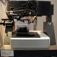
- Arrangement with 20x20x20 mm3 stroke in a case with transportable electronics. This design shows the compact size of the 3D-Nanofinger® and its flexible usage.
- This version is recommended when measurements are required at different places/branches and the ultimate precision is not as important as the portability.
SEM/FIB version
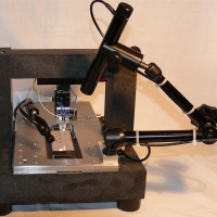
- As part of the Nanoworkbench this version supports linescans and 3D scans within elctron microscopes. The 3D-Nanofinger® is so compact that it can be installed even in a scanning electron microscope (SEM) and a focussed ion beam chamber (FIB).
- The metrology features of a SEM are then expanded to the third Dimension. In particular in a FIB the 3D-Nanofinger® can determine how deep a structure is, immediately after it was produced by the ion beam of the FIB.
Testing bench version
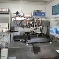
- The universal testing benches allow product development, prototyping, reverse engineering, measurement & quality control, failure detection & analysis with only one system and in until now unknown precision. The accuracy of the base stage is better 50 nm.
- This modular system can include all application packeges like: nanomanipulators, nao probing, force sensors, indenters, inspection Systems.
Micro production version
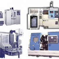
- The 3D-Nanofinger® can also be included in all of our micro production Systems. Those can have up to 16 degrees of movement, several micro-gripper, micro adhesive bonding technology, a 4 axis path control system, 6 video microscopes for pattern recognition and automatic microassembly.
- The 3D-Nanofinger® adds a valuable topography and scouting system to ensure reliable automation.
The 3D-Nanofinger®
- covers the features of Profilometers and 3D Coordinate Measuring Machines by three equivalent axes of movement and measurements along a path, not only along one axis – with a resolution of single Nanometers on Centimeters of stroke.
- detects a contact with its sensor vertically and sidewise: fully 3D.
- measures 3D-profiles, inner and outer contours, dimensional features as well as surface roughness, also sidewise.
- overcomes the restrictions of Profilometers, Coordinate Measuring Machines and AFMs.
- is part of our Nanorobotics and can be integrated in all our systems, freely programmable from point operations to complete measurement tasks.
- 3 axes with 10 – 50 mm stroke in xy and 10-20 mm stroke in z
- 0.5 nm movement resolution
- 2 nm position sensor resolution
- scan resolution up to 2 nm (setup dependent)
- Nanofinger® probe tips can have different shape, hardness and a radius from 50 nm up to a few mm, e.g. to operate as manipulation tool
- 1d measurements as Scout
- 2d measurements for linescans
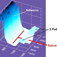
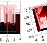
- 3d topography measurements for coarse and fine sample structures
- dimensional measurements in all directions
- automation on many different levels, also within other processes
- Adding 3D to conventional SEM or FIB surface imaging information – In situ Surface Sensing and Nanoprofilometry for Focused Electron and Ion Beam Induced Processes Verification
Andre Linden, Frank Nouvertné, Axel Rudzinski, Torsten Michael, Mark Levermann, Eva Maynicke
Download PDF - 3d Nanofinger
Raith GmbH
Download PDF - eLINE Plus
Raith GmbH
Download PDF
Principle of operation
- The Nanofinger® sensor is a small MEMS device that detects the distance between its probe tip and a sample. In a distance of about 10 nm the Nanofinger® sensor detects the sample by measuring the Van-Der-Vaals forces between sample and tip – without touching the sample.
- The Nanofinger® sensor is driven by a special high speed electronics that reacts with a bandwidth of several KHz. The Nanofinger® sensor is moved towards a sample in closed loop with 1 nm increments until it reaches the desired signal value (e.g. at 75% amplitude). At this moment the position of the stage that moves this sensor is stored as coordinate data. The Nanofinger® sensor is removed again and then moved aside for the next approach, at any time in closed loop with 1 nm increments, in any direction X, or Y or Z over Centimeters stroke.
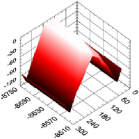
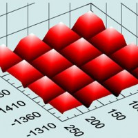
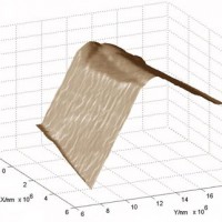
- Since all movement axes of the 3D-Nanofinger® offer 1 nm movement resolution, it is easy to prepare a 3d image by making arrays of Linescans.
Flexible usage
- The 3D-Nanofinger® is one module of our Nanorobotics and can be moved and programmed just as any other sensor or actuator in the system.
- As a module the 3D-Nanofinger® can be used stand-alone or inside of Nanorobotics and micro production systems or e.g. CNC machines.
- Within the “Nanoworkbench” from Klocke Nanotechnik the 3D-Nanofinger® can be used in any SEM/FIB system as “Scout” to guide other tools to the sample or for 3d Topography measurements. A “Live Image Positioning” module directs the Nanofinger® in xy to the target point just by mouse-click into the SEM Image.
- The Nanofinger® can be programmed by simple teaching like all other tool of the system, e.g. for Scouting, for finding a maximum point on a sample measure the height or guide an electrical probe there. Even full 3d-profiles can be parts of a bigger process.
®: Nanofinger is a registered trademark of Klocke Nanotechnik GmbH, Aachen

